
Introduction of Rigid PCB
The inventor of the printed circuit was the Austrian engineer Paul Eisler, around 1943, the USA began to use the technology on a large scale to make rugged radios for use in World War. Before printed circuits (and for a while after their invention), point-to-point construction was used. For prototypes, or small production runs, wire wrap or turret board can be more efficient. Predating the printed circuit invention, and similar in spirit, was John Sargrove’s 1936-1947 Electronic Circuit Making Equipment (ECME) which sprayed metal onto a Bakelite plastic board. The ECME could produce 3 radios per minute.
The PCB is substrate for assembling electronic components, which is printed board forming point-point connection on universal substrate according to pre-design, PCB is the basic part of electronic product and it is also called “the mother of electronic product”. Its main functions include: bearing electronic components, transmitting power-supplies and signals, isolating and refrigerating. At the same time, it is a very essential and non-substituent connector as substrate for bearing electronic product, which has widely uses, covering consumptive electronic products, softwares, information, telecommunications, medical apparatuses and space fights etc. It could be used for household electrical apparatuses, cash registers, personal computers, TV-sets, VCD, recorders radios, commercial banks, faxes, CT scanners, AV-electrical apparatuses, refrigerators, coolers, washers, printers, automatic sellers, multi-telephones and electronic assemblies.
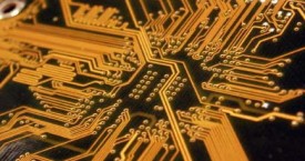
The printed circuit consists of conducting layers and insulating layers, conducting layers are made of thin copper foil, and insulating layers dielectric are typically laminated together with epoxy resin prepreg. The board is typically coated with solder mask. There are quite a few different dielectrics that can be chosen to provide different insulating values depending on the requirements of the circuit. Thermal expansion is an important consideration especially with BGA and naked die technologies, and also glass fiber offers the best dimensional stability.
Its manufacture is prepared by etching, that is majority of printed circuit made by bonding a layer of copper cover the entire substrate, sometimes on both sides, laminating, drilling, being performed by automated drilling machines with placement controlled by a drill tape or drill file, plating, coating, solder resisting, screen printing, testing, assembling, protecting, packaging,designing, safety certifying and cordwood constructing. The materials of PCB are composed of conductive ink and heavy copper, laminate materials are made from BT-Epoxy, composite epoxy material, cyanate Ester, FR-2, FR-4, polyimide and PTFE.
